Precise milling thins PC chips to bring defects to light
An adapted CNC milling machine exposes defects by removing the silicon that encases computer chips.
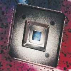
The Hypervision system thinned this computer chip from the backside. The automated operation removed black plastic, the metal paddle on which the chip rests, and much of the silicon of the chip itself.
Hypervision adapted the Emco Maier PCmill 50 to remove plastic, metal, and silicon from the backside of computer chip packages for inspection. Hypervision markets the mill as the Chip UnZip.
When a computer chip fails during manufacture, the defect can be located by a powerful emission microscope that detects a minute amount of light emanating from the defect. But, before the microscope can detect the faint failure-emission, most of the hard, brittle silicon encasing the chip must be precisely removed.
Most newer computer chips are about 700 µ (0.03 in.) thick, and most of the silicon has to be removed from the back of the chip—back thinned— to let the light emissions shine through the remaining silicon.
From milling trainer to PC shaver
Failure analysts at semiconductor plants around the world tried to invent methods for back-thinning chips. They found it was very difficult not to crack the chips (which meant they could not be tested); even when they didn't crack the chips, they often destroyed the chip's leads (again eliminating the possibility of testing).
A California company—Hypervision Inc., which designs and manufactures emission microscopes—finally found the answer in the adaptation of a computer numerically controlled milling machine—the Emco Maier PCmill 50. The machine could remove the backside plastic and metal die paddle (both fairly easy to work with), and then the brittle, hard silicon. Its precision can control the depth of the window being cut into the back of the silicon to within a few ten-thousandths of an inch. And it has highly dependable repeatability so every IC package of a given type can be opened in exactly the same way.
Using special cutting tools, this precise milling machine rapidly removes the plastic and metal die paddle from the backside of the computer chip's package. Then, switching to a diamond-coated tool, it removes the silicon of the chip itself. The machine's computer numerical controls maintain precise accuracy in the X, Y, and Z dimensions. Also, the machine is automated, so a technician needs to enter only occasional keyboard instructions to control the process.
Surprisingly, Emco Maier PCmill 50 was originally designed as an automated milling machine for training purposes—not for industrial production. Although small in size, the PCmill 50 has the same ruggedness and precision as Emco Maier's larger machines. The combination of small size and high reliability are well suited to semiconductor manufacturing where available floor space is limited and very expensive.
Marketed by Hypervision as Chip UnZip, the machine offers variable spindle speeds, required because of the differing materials in a semiconductor package, and tools that can be changed quickly. Its ability to be "homed" to a reference position quickly and automatically is an important feature when the target area on the semiconductor devices is very small and when reproducibility of operation is critical. The machine's enclosure is interlocked with its drive motors, a safety feature mandatory in semiconductor environments.
A personal computer controls the PCmill 50. The controlling software is the same used on large Emco Maier machines and permits the user to assemble libraries of commonly used command sequences. Semiconductor failure analysts using the machines create a library for each type of device they thin.
Flexible PC solutions
No one knew it at the time, but the introduction of the PCmill 50 into the semiconductor community would solve not just one but several problems. In addition to using the machine to thin the backside of chip packages to locate light from defects, some chip makers are thinning the backside and then using acoustic microscopes, which use ultrasound, to nondestructively image internal features. With most of the silicon removed, acoustic microscopes can make extra-sharp images. Other manufacturers are removing all of the chip's silicon so they can optically examine the chip's leads.
Another application for the precision silicon-removal technique involves chips cut from circular wafers. Each wafer may contain hundreds of chips, so wafers are expensive. Since it is beneficial to find defects as early in the production process as possible, chip makers have long wanted to be able to thin the backside of wafers. Until the PCmill 50 technique was developed, this meant slowly lapping the backside of the entire wafer, which may be several inches in diameter. When lapping was completed, engineers had a circle of silicon only a few thousandths of an inch thick. Such lapped wafers often break before they can be tested. PCmill 50 solves this problem by letting engineers back thin single chips on the wafer. The process is much faster and safer than thinning the whole wafer, and can be repeated for additional chips on the wafer, if desired.