Photochemical Etching – and How It’s Done
Photochemical etching is a machining technique that leverages the principles behind photography to shape a piece of sheet metal and turn it into a finished product or component.
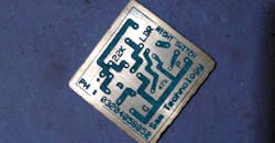
The modern form of industrialized photochemical etching arose in the 1960s during a boom in printed circuit board (PCB) manufacturing. The demand for computer processing power was rising rapidly, and manufacturers needed a way to print highly precise and thin components quickly and inexpensively.
However, it’s thought that the mechanics of the photochemical machining technique date back thousands of years to jewelry-makers in Egypt.
The advent of photochemical machining brought an explosion of innovation in several industries. What exactly is it? And how does it work?
What is the photochemical etching process?
The photochemical machining (PCM) or photochemical milling process uses photoresist imaging to place a pattern on top of a metal workpiece. This pattern is then used to invoke selective corrosion, thereby efficiently removing areas of the component or product and shaping it as desired.
Some of the market segments making widespread use of photochemical etching include the life sciences, medical device manufacturing, and aerospace and automotive industries. Electronic devices and their components, such as circuit boards, also feature products manufactured this way.
Here is a summary of the production steps.
1. Prepare the metal. Preparing the metal begins with choosing the sheet thickness and type – most commonly titanium, steel, aluminum or copper. Certain alloys offer greater corrosion resistance than others.
Preparation continues with cutting the workpiece to an appropriate size and shape for the work, and then decontaminating the surface of any grease or particulates.
2. Create the photo tool. Next comes creating the overlay for photoresist imaging. This begins with a CAD drawing which, when finalized, is printed onto the photo tool made from polymeric film.
This step includes undercutting. The photochemical process’s footprint will be larger than the intended pattern when it takes effect. Therefore, the digital drawing and photo tool must be larger than the targeted size to achieve the correct dimensions.
3. Laminate the metal. Step three involves coating the sheet metal with photoresist film. This polymeric layer is where the photo-sensitive materials and photo-initiators are located.
4. Print, expose, and develop. The image from the CAD drawing – the photo tool with the desired shape – is transferred onto the sheet-metal workpiece, which remains coated with photoresist film. This step involves applying UV radiation. The photoresist film commences a chemical reaction where any portions of the sheet metal not protected by the photo tool undergo polymerization.
As promised with the comparisons to photography, this is the step during which the patterned metal is “developed.” The areas that have not undergone polymerization in the previous stage have become softened and can be washed away with an alkaline solution. The rest of the pattern is unaffected, which leaves the newly shaped workpiece behind.
5. Etching, stripping, and inspection. Lastly, etching – the process of removing the softened metal – takes place. Specialists apply an etching solution using a chamber and spray tools. It reacts with the metal at the atomic level to quickly dissolve the weakened material and leave behind the desired “developed” portion of the pattern.
The final step, stripping, involves applying another alkaline solution to remove the photoresist film from the surface.
Visual inspections and highly precise measurements ensure the parts meet the desired specifications.
Why is photochemical etching useful?
The primary draw of photochemical machining or etching is the high level of precision it achieves compared to other techniques. Many niche-specific products and components are too thin and detailed to manufacture in any other way. Modern photochemical etching can produce features as small as 25 microns across and with tolerances around 10 microns.
The level of accuracy and detail offered by photochemical etching makes it a preferable alternative to metal stamping, water jet cutting, punching and EDM (electrical discharge machining) for the thinnest of thin-gauge parts.
In addition to being highly precise, manufacturers and customers also benefit from the process’s low cost and high speeds relative to other techniques.
Other advantages of photochemical machining include:
• Extremely fast prototyping
• The ability to make quick design changes during mass production
• Leaving behind no burrs or sharp edges
• Taking just hours to produce an item after receiving technical drawings
The only true limiting factor to photochemical milling’s usefulness is workpiece thickness: Depending on the metal selected, the raw material can be no more than 6 millimeters thick – and sometimes even thinner, in the case of copper. Other techniques, like punching, waterjet cutting or a combination of these processes, may be required for any greater thicknesses.
Despite these limitations, photochemical machining finished parts can be extremely sophisticated or intricate – and with virtually no limit to the complexity of the design.
Real-world photochemical etching applications
It’s not surprising to find photochemical etching applications in numerous industries due to its roots in printed circuit board manufacturing. The digital revolution finds every company doing business online, and there are billions of appliances, mechanisms, and devices receiving Internet of Things (IoT) upgrades – meaning computing power is required just about everywhere on Earth.
Big Data and advanced computing applications aren’t the only areas of manufacturing benefitting from photochemical etching, however. Some others include:
• Aerospace and automotive
• Medical devices and implants
• Household and commercial appliances
• Fuel cells and motors
• Custom seals and gaskets
• Screens and extremely fine filters
• Home and yard décor
• Semiconductors, computer processors and sensors
• Electromagnetic (EM) and radiofrequency (RF) shields
Nontraditional no longer
Photochemical etching is still considered a nontraditional manufacturing process, but that’s changing quickly, given the process’s widening deployment and expanding number of applications. It has both those factors in common with 3D printing, which similarly is beginning to experiment with nanoscale fabrication.
Thanks to its precision and efficiency, as well as its ability to produce components at the nanoscale, photochemical machining will continue to gain recognition as manufacturing evolves.
Emily Newton is the Editor-in-Chief of Revolutionized, an online magazine exploring the latest industrial innovations.
About the Author
Emily Newton
Emily Newton is the Editor-in-Chief of Revolutionized, an online magazine exploring the latest industrial innovations.